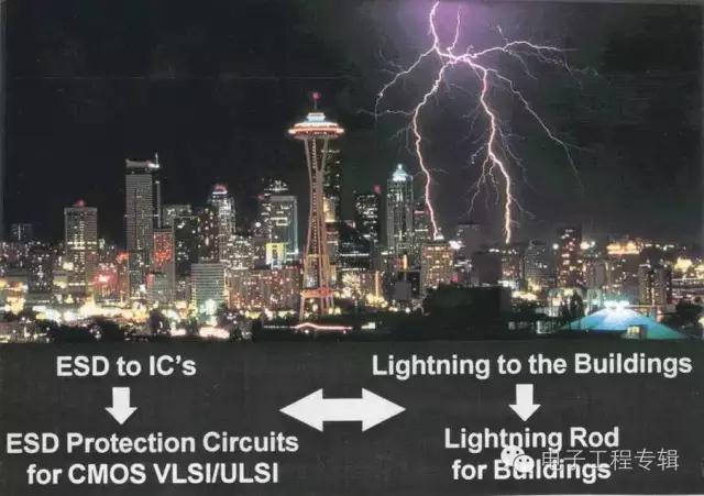
Electrostatic Discharge (ESD: Electrostatic Discharge), should be all Electrical Over Stress) damage caused by the main culprit.Because electrostatic usually transient voltages or integrated circuit system caused by excessive electrical stress (EOS: very high (> a few kv), so the damage is devastating and permanent, will cause the circuit directly burned. So to prevent electrostatic damage is all the IC design and manufacture of the number one problem.
Electrostatic, usually produced artificially, such as production, assembly, testing, storage, handling and is likely to be made in the process of electrostatic accumulated in human body, instrument or equipment, even the components will accumulate static electricity, when people unwittingly make the charged object contact will form the discharge path, instantly making electronic component or system was damaged by electrostatic discharge (this is why the previous computer must wear electrostatic ring at the work table, prevent human electrostatic damage chips), as the electric charge stored in the cloud in an instant a dramatic lightning through the clouds, the earth would open, and usually are coming on a rainy day, because the big easy to form a conductive to air humidity.
So, how to prevent electrostatic discharge damage?First of all, of course, change the environment from the source to reduce static electricity, such as reducing friction, less wear wool sweater, the control air temperature and humidity, etc.), and of course this is not our heavy point of the discussion today.How we are going to discuss today when involved in circuit protection circuit, when the outside world have electrostatic our electronic components or systems to protect themselves to avoid being electrostatic damage (in fact is to install a lightning protection needle).This is also a lot of IC design and the manufacturer´s problem, many companies have a special design of ESD team, today I and everybody from the most basic phase in interpretation of the theory of ESD protection principles and attention points, you will find/speak in front of the PN junction diode, transistor, MOS tube, the snap back all...
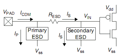
Previous thematic interpretation theory of PN junction diode, just speak: the diode has a characteristic is to the reverse blocking (don´t remember to turn in front of the class), and reverse bias voltage continue to increase the Avalanche Breakdown happens (just Breakdown) and conduction, we call it a Clamp diode (Clamp).This is what we need for the theoretical basis of design of electrostatic protection, we just use the reverse cut-off characteristic make the bypass in normal work in the off state, and the outside world is static electricity when the bypass diode avalanche breakdown and form the bypass circuit to protect the internal circuit or grid (whether similar to sink a weir in the home, prevent floods left the tap off the whole toilet).So the question comes, the breakdown of the protection circuit is completely dead?Could it be a one-off?Of course, the answer is not.P-n junction breakdown points of two kinds, respectively is the electric breakdown and thermal breakdown, electric breakdown is referring to the avalanche breakdown (low concentration) and zener (high concentration), and the electric breakdown is the main carrier collision ionization produced new electronic - hole (electron - hole), so it is recoverable.But thermal breakdown is irreversible, because heat gathered in silicon (Si) was burned down by the melting.So we need to control in the conduction of the instantaneous control current, typically in protecting diode and a high resistance in series, in addition, we can also understand why is not ESD area is not the form of Silicide?And give everyone a theory, ESD is usually in the chip Pad at the input side, and not inside the chip, because we always want to the outside world of electrostatic need to discharge off the first time, in it there will be a delay (pay attention to my previous anatomy next to the chip Pad have diode http://ic-garden.cn/?p=482).There are even put two levels of ESD, reach the purpose of double protection.
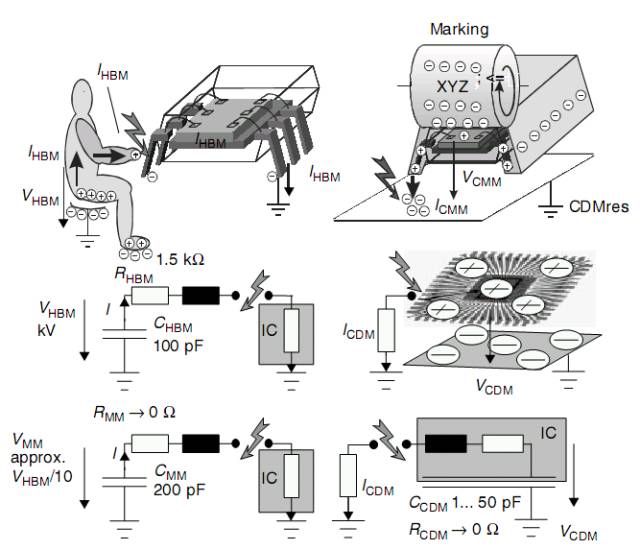
Before about ESD principle and Process, we first under ESD standard and test method, according to the way of static electricity generation as well as to the damage mode of the circuit is usually divided into four different test way: Human Body discharge Model (HBM: the Human Body Model), Machine discharge mode (Machine Model), element charging mode (CDM: Charge - Device Model), the electric Field induction Model (FIM: Field - Induced Model), but the industry usually use the first two models to test (HBM, MM).
1, ,Discharge body model (HBM) : friction, of course, is the human body has a charge suddenly encounter release charge led chip burned breakdown, autumn touch with people often get an electric shock it is for this reason.Industry also has A track record of HBM ESD standard (3015.7 MIL - STD - 883 - c method, equivalent body capacitance is 100 pf, equivalent body resistance is 1.5 Kohm), or international electronics industry standards (EIA/JESD22 - A114 - A) also has A regulation, to see which one will you follow.If it is 3015.7 MIL - STD - 883 - c method, it provides less than < 2 kV for Class 1, 2 kV ~ 4 kV for Class - 2, 4 kV ~ 16 kV for Class - 3.

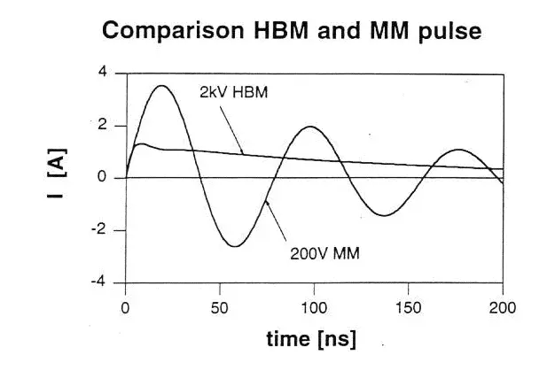
2,Discharge, machine model (MM) : of course, is A machine, such as robot move produce electrostatic touch chips by pin feet release, standard of EIAJ - IC - 121 method of twenty (or standard EIA/JESD22 A115 - A), equivalent machine resistance of 0 (metal) because it is over, capacitance is still 100 pf.Because the machine is a metal and resistance to 0, so the discharge time is short, almost is ms or between us.But the more important question is, as a result of equivalent resistance to 0, so the current is very big, so even 200 v the MM of discharge is greater than 2 kv HBM discharge damage.And the machine itself because there are a lot of wires produce coupling each other, so the current will change with time change and interference.
ESD test method similar to the inside of the FAB GOI test, after the specified pin to give him a ESD Voltage, for a period of time, and then come back to test electrical see if it is damaged, no problem to add a step for a period of time, the Voltage of ESD and electrical measurement, so until the breakdown, at this time the breakdown of the critical breakdown Voltage for the ESD Voltage (ESD failure threshold Voltage).We are usually called circuit voltage zaps (3) three times, in order to reduce the test cycle, usually starting voltage using the standard 70% ESD threshold voltage, each step can be adjusted according to the need to 50 v or 100 v.
(1). Stress number = 3 Zaps. (5 Zaps, the worst case)
(2). Stress step Δ VESD = 50 v, 100 v) for VZAP < = 1000 v
Δ VESD = 100 v, 100 v, 500 v) for VZAP > 1000 v
(3). Starting VZAP = 70% of averaged ESD failure threshold (VESD)
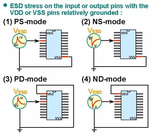
In addition, because each chip pin feet a lot, you are the one pin or pin combination testing, so will be divided into several combination: the I/O - pin test (Input and Output pins), pin - to - the pin test, Vdd and Vss test (the Input to the Output side), Analog - pin.
I/O pins: (1) is respectively to the input pin and the output pin do ESD test, and have positive and negative charge, so there are four combinations: input +, the output and input + negative charge +, the output + negative charge.Test input, output and all other pins floating (floating), and vice versa.
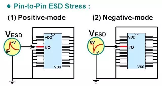
2. Pin - to - pin test: electrostatic discharge occurs between pin - to - pin form a loop, but if you want to test every two feet combination is too much, because if after any I/O to voltage will affect the whole circuit is definitely a VDD/Vss to power for the whole circuit, so the modified with an I/O pin plus the ESD voltage of positive or negative, all other I/O earth together, but the input and output at the same time Floating (Floating).
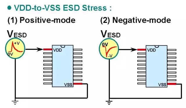
3, Between Vdd and Vss electrostatic discharge: you just need to put the Vdd and Vss, all the I/O of floating (floating), so to electrostatic let him through the Vdd and Vss.
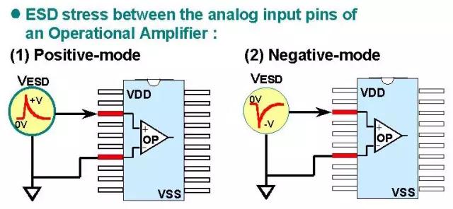
4, The Analog - pin discharge test: Analog circuits because of the many difference than (Differential Pair) or operational amplifier (OP AMP) are two at the input, to prevent a damage result in difference than or operation failure, so you need to do ESD test, of course is only for the two pins, all other pins floating (floating).
Ok, the principle of ESD and test section at this point, go ahead the following Process and design factor
As Moore´s law has narrowed, the size of the device is more and more small, deep more and more shallow, bigger more and more thin, so electrostatic breakdown is more and more easily, and in Advance process, Silicide introduction will let electrostatic breakdown become more acute, so almost all of the chip design to overcome the electrostatic breakdown problem.
Electrostatic discharge protection can solve the Process from a FAB, also can from the IC Design Layout to Design, so you will see an option of ESD Prcess is layer, or the Design rule with ESD Design rules for the customer to choose, and so on., of course, some customers also will according to the SPICE model of electrical through the layout design of ESD.
1, The processes of ESD: either change the p-n junction, or change the p-n junction of load resistance, and can only rely on ESD_IMP change PN junction, and change the load resistance and the p-n junction, is to use non - silicide or the method of series resistance.
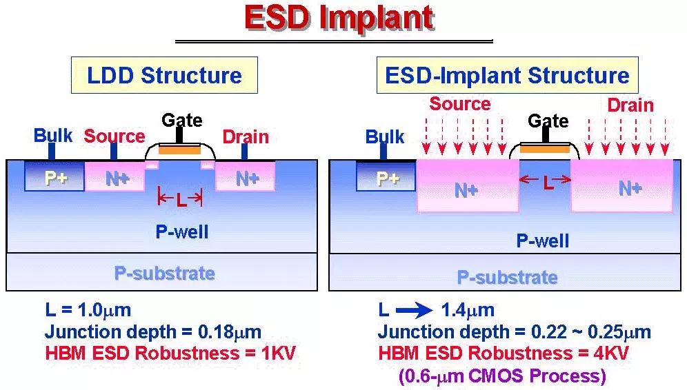
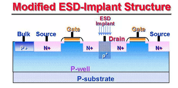
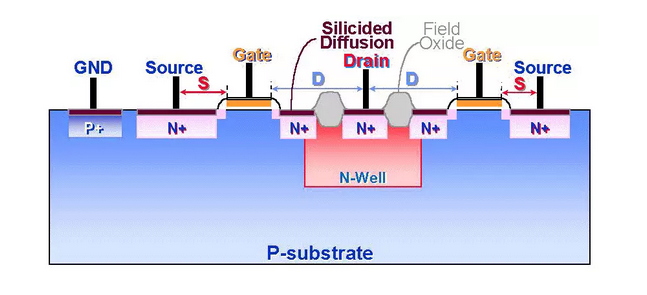
2) Contact hole: (contact) of ESD implant in LDD device of the N + drain hole below a P + b, and depth than the N + drain (drain) tapping depth, so that the original drain breakdown voltage of tapping reduce (8 v -- > 6 v), so can happen in the LDD sharp-angled breakdown from the drain breakdown tapping guide before you walk in order to ensure the breakdown of the drain and Gate tapping.So this design can maintain device size remains the same, and MOS structure did not change, so do not need to extract the SPICE model.Of course the smart for non - silicide process, or you contact also dozen don´t go in implant.
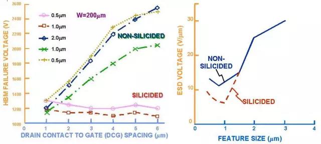
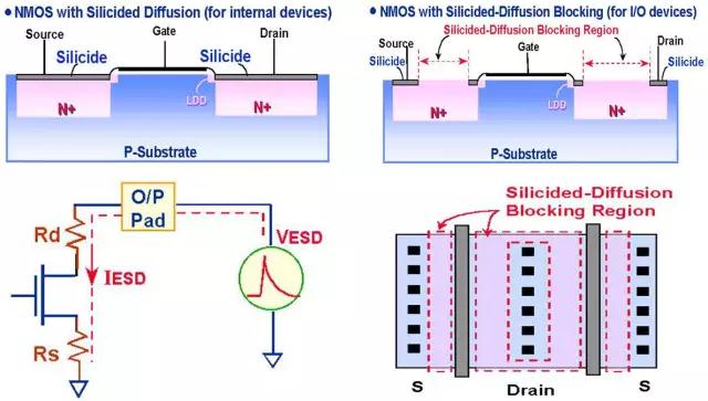
3) SAB (SAlicide Block) : generally we to decrease the interconnection of MOS capacitor, we will use silicide/SAlicide process, but if this device is working on the output side, our device load resistance become low, the ESD voltage will be full load between LDD and Gate structure breakdown damage easily, so the output level of MOS silicide/SAlicide we usually use the SAB (SAlicide Block) mask RPO, blocking don´t form silicide, add a photo layer increased costs, but the ESD voltage can be increased from 1 kv to 4 kv.
4) Series resistance method: this method need not increase mask, should be the most cost-effective, the principle is similar to the third increase resistance method (SAB), I deliberately gave him a resistor in series (such as Rs_NW, or HiR, etc.), so also reached the SAB method.
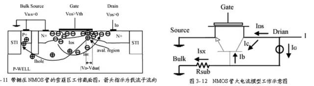
2, In the design of the ESD: it was completely by the designer´s kungfu, some companies in the design rules have been provided to the customer solution, customer just according to drawing, some not only depend on customer´s own designer, many design rules are written, the only guideline/reference is not a guarantee.Are generally the Gate/Source/Bulk short connect together, the Drain junction tapping in the I/O port under ESD surge (surge) voltage, NMOS called GGNMOS (Gate - Grounded NMOS), PMOS called GDPMOS (Gate - to - Drain PMOS) tapping.
NMOS, for example, the principle is the Gate closed, the Source/Bulk PN junction sub zero slants originally, when the I/O side has large voltage, the Drain/Bulk tapping PN junction avalanche breakdown, instantaneous Bulk have big current and substrate resistance formation pressure difference leads to Bulk/Source PN is partial, so the MOS parasitic lateral NPN transistors into put district (launch knot is partial, and collecting the partial), shows so Snap - Back, play a protective role.PMOS similarly is derived.
The principle seems simple, but what is the essence of design (know how)?How to trigger the BJT?How to maintain the Snap back?How to hold the HBM > 2 kv or 4 kv?
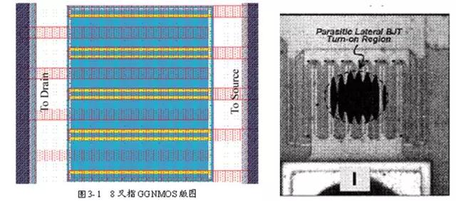
How to trigger?There must be large enough substrate current, so later now more widely used refers to cross in parallel structure (multi - finger).But the structure of the main technical problem is to increase, the base width magnification coefficient decreases, and so the Snap - the back is not easy to open it.And as finger populations, can lead to evenly between each finger it difficult to open, this also is the main bottleneck of ESD design.
If you want to change this kind of problem, there are about two practices (because triger is voltage, improve voltage are either resistance or current) : 1, the use of SAB (SAlicide - Block) in the I/O Drain formed on the tapping of a non - high resistance Silicide region, makes the Drain square resistance increase, and ESD current distribution more uniform, thus improve the discharge capacity;2, increase a P - ESD (Inner - Pickup imp, similar to the above contact hole P + ESD imp), the N + Drain below a P +, tapping reduce Drain the avalanche breakdown voltage of tapping, have more earlier avalanche breakdown current (see literature papers: Inner Pickup on ESD of multi - finger NMOS. PDF).
For the Snap - the back of the ESD has two small common sense to share with you:
1) NMOS we can usually see better Snap - the back features, but in fact PMOS transistor is very difficult to have a Snap - the back features, than NMOS and PMOS ESD resistance characteristics of common good, this truth with HCI effect, mainly because of breakdown time of NMOS is electronic, the mobility is large, so the Isub is very easy to make Bulk/Source wizard, but it is difficult to cough up PMOS transistor.
2) The Trigger voltage/Hold: the Trigger voltage will snap - before, of course, is the back of the first inflection point (Knee - point), parasitic BJT breakdown voltage, but also between BVCEO and BVCBO.And Hold the voltage is to sustain continuous ON the Snap - the back, but can not enter the gate lock (Latch - up), or enter the secondary breakdown was damaged (thermal breakdown).Is the secondary breakdown current has a concept, is entering the Latch - heat up after the I ^ 2 * R in silicon melting, and this is current limit, can control the W/L, or adding a current limiting high resistance, the easiest and most commonly used method is widened Drain distance/tapping away SAB (ESD common practices of rule).
3, Grid coupling (Gate - picking) ESD technology: we just talked about, Multi - finger the uniformity of the bottleneck of ESD design is open, suppose you have 10 finger only, and in the ESD discharge occurs, the ten finger will not necessarily at the same time conduction (typically due to Breakdown conduction), common to only 2-3 finger will guide, this is because the layout is unable to get the relative position of each finger, and pull the same direction, the 2 ~ 3 finger a conduction, ESD current focus to this 2 ~ 3 a finger, while the other finger is still kept closed, so the ESD protection ability is equivalent to only 2 ~ 3 finger protection, rather than ten finger protection.This is why the component size has done a lot, but the ESD protection ability is not the main reason for the rise, as expected, and the wire area is not expected to bring ESD enhancement, how to do?Actually very simple, is to reduce the Vt1 (the Trigger voltage), we through the way of increase grid voltage, substrate to open instead of breakdown and conduction substrate current generated in advance, then can let other finger also open into conducting state, let each finger under ESD current, really play a role of a large area of ESD.
But this GCNMOS ESD design has a disadvantage is that the channel opens the breakdown, easy to cause the current grid oxygen so he missing is a kind of very good ESD design scheme, and the source area is smaller, the greater the influence of grid voltage, and the active area, the greater the snap back - the more difficult it is to open, so it is difficult to grasp.
4, There is a complex of the ESD protection circuit: Silicon Controlled thyristor (SCR: Silicon Controlled Rectifier), it is what we talked about before PNPN structure of CMOS parasitic trigger Snap Back and Latch - up, through the ON/OFF to realize the protection of circuit, we can review, as long as the previous inside that inhibit the factor of Latch - up thought it is ok to let it happen, but can only apply to the Layout, may not apply to the Process, otherwise the Latch - up to fail again.
|