Schottky diode is precious metals (gold, silver, aluminum, platinum, etc.) A is positive, negative for N type semiconductor B
Use the contact form on the surface of the potential barrier rectifier characteristics and made of metal - semiconductor devices.Due to the
For there are a lot of in the n-type semiconductor electronics, only very small amounts of free electrons in the precious metals, so Electrons from the high concentration of B to spread in A low concentration., of course, no hole in A metal, and there is no hole diffusion movement from A to B.Along with the continuously from electronic spread to A, B, B surface electric electron concentration gradually reduce, electrically neutral surface was damaged, then form A barrier, the electric field direction for B to A.But under the electric field effect, also can produce the electrons in A drift motion from A to B, from the weakened due to the motion of the spread form of the electric field.When establishing a certain width of the space charge region, different electric drift motion of electrons and the concentration diffusion reach the balance of relative movement of electrons, it forms the schottky barrier.
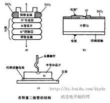
Schottky diode structure schematic diagram
ypical schottky rectifier circuit inside the structure based on n-type semiconductor substrate, in the above form with arsenic dopant of N - epitaxial layer.Anode using molybdenum or aluminum material blocking layer.Using silica (SiO2) to eliminate the electric field at the edge of the area, improve the withstand voltage value of the pipe.N-type substrate have a very small resistance, its doping concentration is 100% higher H - layer.Formed in the substrate below the N + cathode layer, its function is to minimize the contact resistance of the cathode.By adjusting the structure parameters, N type formed between substrate and the anode metal schottky barrier, as shown.When on both ends of schottky barrier and forward bias (anode metal positive, n-type substrate to connect power cathode), narrow schottky barrier layer, its resistance decreases;On the other hand, if on both ends of schottky barrier and reverse bias, schottky barrier layer is wider, its internal resistance.
The place on put together is narrated, the structure principle of schottky rectifier rectifier with PN junction there is a big difference in the PN junction rectifier is usually referred to as "rectifier tube, and the metal - half a catheter tube was called schottky rectifier tube, using silicon planar process manufacturing aluminum silicon schottky diode has appeared, this not only saves precious metals, reduce the cost, also improve the consistency of the parameters.
|