一、The working principle of field effect tube - concept
Field effect tube (FET) is a field effect transistor (field effect transistor), because it only on the majority carrier conductive semiconductor, also known as single polarity field effect tube, is a common use of the input circuit of the electric field effect of a loop current to control the output voltage control semiconductor devices, field effect tube not only has a bipolar transistor advantages of small volume, light weight, long service life, and the input circuit resistance up to 107 ~ 1012 Ω, low noise, good thermal stability, strong ability to resist radiation, and power saving than the latter, these advantages make it since the 1960 s was born is widely used in various electronic circuits.
二、Working principle of field effect tube structure
All the FET gate g (gate), drain d (drain) tapping, the source (source) s three pole, corresponding to the base of the bipolar transistor b (base), c (collector) and emitter collector e (emitter).Besides junction field effect tube, all of the FET has the fourth side, is called the body (body), base (base), block (bulk) or substrate (substrate).P and N area boundary surface depletion layer formation, and the source and drain d s non depletion layer between the area known as conductive channel.
三、The working principle of field effect tube - classification
Field effect tube can be divided into junction field-effect tube type (jfets) and insulated gate field-effect tube (JGFET), junction field-effect tube (jfets) the name, because there are two PN junction type insulated gate field-effect tube (JGFET) for grid with other electrode insulated completely the name.Because type insulated gate field effect tube grid for aluminum, so it is also called the MOS tube.
Field effect tube according to the different methods of conductive to differentiate, can be divided into depletion and enhanced.When the grid voltage is zero have larger drain current called the depletion mode;When grid voltage is zero, the drain current is zero, also must add after the grid voltage is called enhanced drain current.
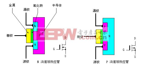
Whether junction field-effect tube type or insulated gate field effect tube, whether depletion mode field effect tube or enhanced field effect tube, can be divided into N channel and P channel, its structure, respectively as shown in the figure below:
四、Working principle of the field effect tube junction
Junction field-effect tube can be divided into N channel junction field-effect tube and P channel junction field-effect tube, let´s with N channel as an example to show the working principle of the junction field effect tube.
In order to ensure the N channel junction field-effect tube can work normally, should be in the grid - plus negative to the voltage between the source (i.e., uGS < 0), to ensure the depletion layer under reverse voltage;In between - leakage source forward voltage uDS, to form a drain current.Grid - the greater the negative voltage between the source and the PN make depletion region formed by the interface of the more thick, the narrower the conductive channel, the channel resistance, the smaller the drain current iD;On the contrary, if the grid - the smaller the negative voltage between the source and the depletion region is more thin, conducting channel is wide, the channel resistance decreases, the greater the drain current iD.Thus realized the field effect tube grid between negative voltage source and the control of the channel current.
For P channel junction field-effect tube, similar to N channel principle, but to be between the gate and the source and forward voltage (i.e., uGS > 0) to ensure that it can work well.
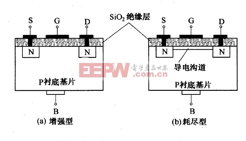
五、The working principle of the field effect tube - insulated gate type
With n-channel depletion MOS tube, for example, if made in MOS tube, incorporating a large number of positive ions in the SiO2 insulation, so even if the uGS = 0, under the effect of positive ions p-type substrate surface is inversion layer, the conductive channel between leak - source.As long as the leak - between the source and the forward voltage, can produce drain current, and uGS for timing, inversion layer grows wider, the channel resistance smaller, channel current iD;Otherwise, uGS is negative, the narrow inversion layer, the channel resistance, iD.When uGS from zero to a certain value, the inversion layer disappears, leak - conductive channel between source disappear, iD = 0.Implements the gate source voltage control of the drain current.
六、The working principle of the field effect tube - enhanced
N channel, for example, in a n-channel enhancement mode device, should add forward voltage between the gate.Positive voltage attracted body of freely moving electrons from moving grid, formed the conducting channel.But first of all, good electronic area need to be attracted to the grid against doping ions in FET;It formed a carrier without movement known as exhausted area, this phenomenon is called the threshold voltage of the FET.Higher gate voltage will attract more electrons through the gate, will create a conducting channel from the source to the drain;This process is called "trans."
七、The working principle of the field effect tube - - depletion
In a n-channel depletion model device, between gate plus negative voltage will lead to a depletion region to expand the width, from the border into the channel, so that the narrow channel.If the depletion region extended to completely shut down the channel, the channel resistance between the leakage source will become big and FET would like switch shutoff.Similarly, in a P channel depletion model stage of devices, between gate and forward voltage will make the channel width and channel resistance smaller, made the current are more likely to pass.
|